Dark & matched blank
Record detector background and the holder/substrate reference. Keep alignment, probe intensity and timing fixed.
OPTICAL INSTRUMENTATION / TU ILMENAU
The goal: use light to change a polymer sample’s optical response, then measure that change. Start with the working illumination unit and explore the two proposed readout methods.
Loading the supplied CAD geometry…
Drag to rotate · Scroll to zoom · Geometry from supplied 3MF files. Exploded spacing is for explanation.
The excitation LEDs illuminate the sample. Detector readings are excluded from this stage.
Functional diagram, not a wiring or fabrication drawing. Final geometry depends on the specimen.
Compare a matched blank with the specimen before and after exposure.
Synthetic spectral shapes for explanation only. They are not DASA, spiropyran or azobenzene measurements.
TRY THE MEASUREMENT PRINCIPLE
Generic examples, not models fitted to a named material.
PWM setting is illustrative; it is not calibrated irradiance.
Ready0.0 s
3× playback. The plotted time is simulated experiment time.
No hardware is connected. CSV exports are explicitly marked as simulated.
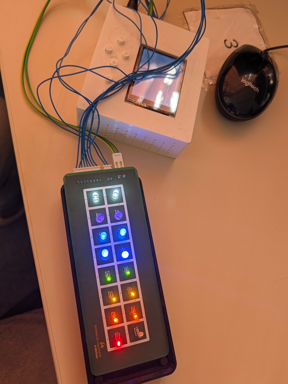
Project photograph supplied by Amey. Visible LED colours do not establish calibrated emission wavelengths.
FROM BUILD TO MEASUREMENT
My internship at TU Ilmenau investigates an LED-based lighting module for photoswitching on polymer surfaces. My latest build work includes developing and assembling the LED PCB, programming the Arduino control and designing a new enclosure, using Xu Li’s earlier system as a reference.
The supplied CAD files shown above come from that reference design. They help explain the construction and are not presented as a verified CAD record of every change in my rebuilt unit.
Updated 6 October 2026 · hardware status based on Amey’s latest project report.
ENGINEERING NOTES
The source KiCad layout and firmware show 16 LED positions, eight PWM columns and two row-enable lines. A PWM value controls switching duty cycle; it is not a measured optical power.
| Function | Documented / proposed connection | Status |
|---|---|---|
| LED PWM columns | D10, D9, D8, D7, D6, D5, D4, D3 | Documented source mapping |
| Group enable | D30, D32 | Documented source mapping |
| Six buttons | A6–A11 | Documented source mapping |
| TFT display | D22–D29 data; A0–A4 control | Requires matching display-library configuration |
| OPT101 output | A12 candidate input; common ground | Verify actual package/module and free pin before wiring |
| Probe control | A13 candidate output through a suitable driver | Driver, LED current and wiring to be confirmed |
| Computer logging | USB serial; prepared CSV workflow | No measured dataset yet |
Use the real detector’s documentation for supply, pinout, decoupling and output range. Module terminal names are not bare-chip pin numbers. The requested 100 nF and 1 µF parts and the weak probe source require confirmation before assembly.
The original design allowed intended wavelength-specific emitters, but demonstration LEDs were substituted for cost and timing reasons. Do not infer eight verified wavelengths from the board layout or LED colours.
Record detector background and the holder/substrate reference. Keep alignment, probe intensity and timing fixed.
Check sensor response, settling and ADC headroom. Subtraction cannot repair saturation or a rapidly changing background.
Use probe-only, temperature and repeat-cycle controls to distinguish switching from drift or readout-induced change.
Compare time-resolved readings with suitable UV–Vis measurements. No single voltage value proves a molecular mechanism.
DASA, spiropyran and azobenzene are candidate families discussed for the project. The actual derivative, polymer matrix, excitation band, probe band and reset protocol need specimen-specific agreement. Universal compatibility has not been demonstrated.
The virtual experiment uses a generic first-order response and recovery, an illustrative transmission-to-voltage mapping, and a nominal 10-bit / 5 V ADC. Rates, noise, contrast and exposure settings are chosen only to explain the measurement. The probe is assumed non-perturbing, and background is assumed nearly constant within a reading pair.
The spectral graph is an independent synthetic example, not a spectrum reconstructed from OPT101 voltages. For appropriate transmission measurements, T = I/I₀ and A = −log₁₀(T); a raw OPT101 voltage is not automatically absorbance.
The interactive meshes are converted directly from ledUnterteil.3mf, ledDeckel.3mf, Unterteil.3mf and Deckel.3mf supplied with the Xu Li reference project. LED centres come from the supplied PCB_LED_terminal_v7.kicad_pcb. Electronics, sample and optical paths are explanatory representations; final assembly and measurement dimensions require checking.
The source archives include Bambu Studio print-profile metadata. Meshes retain their source dimensions; placement and exploded spacing are changed for the presentation. The original files remain unchanged.